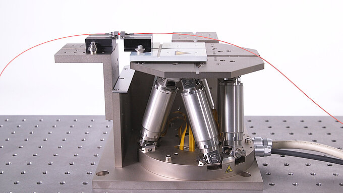
The assembly and packaging of photonic devices requires highly efficient production systems. To technically realize the complex automation tasks in silicon photonics applications, PI has developed various solutions that are essentially based on two pillars: High-precision mechanical positioning systems and algorithms developed, e.g., to find first light or to perform gradient searches that continuously track the maximum signal transmission.
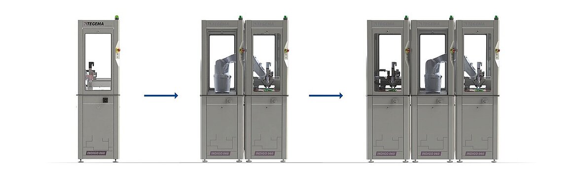
TEGEMA, the multidisciplinary system integrator that is now part of Etteplan, has developed a modular machine platform based on this technology. It is used for the automated assembly of optical components, in particular photonic integrated circuits (PICs). The system works with submicron precision and, thanks to its intelligent architecture, can grow from tasks in research and development of PICs to their series production. It offers cycle times that are ten times faster than current solutions on the market. While up until now testing and packaging of PICs used to take five to twenty minutes, TEGEMA’s platform provides a fully assembled component, including active alignment and fiber termination, in about 30 seconds. Positioning typically takes only fractions of a second.
The lack of such a solution has so far hampered the market for photonic components. In a way, with this platform, we have now created the missing link between the front end and the back end: a real breakthrough for integrated photonic circuits.
Arno Thoer, Director Technology & Engineering at TEGEMA
PI and TEGEMA Combine Competencies for Maximum Speed
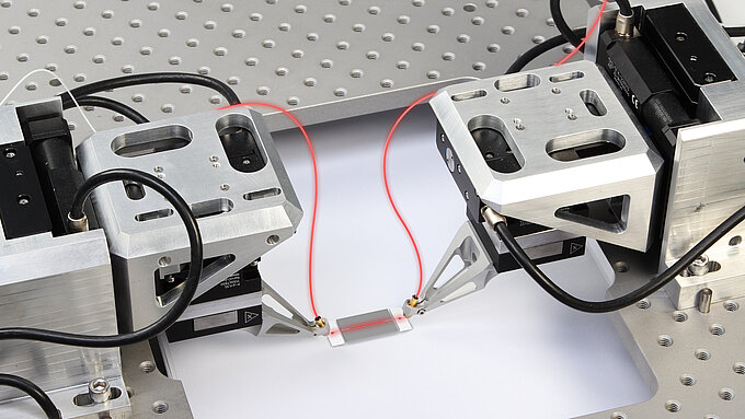
The machine is based on TEGEMA's modular platform architecture, which allows the connection of hardware modules specific to the application at hand. For testing and packaging of PICs, the machine vision systems for rough positioning, an adhesive dispenser, a UV light source for curing the adhesive, and a rotation platform are used to transport the individual elements and, consequently, the finished components. At the heart of the photonic assembly platform are ultrafast and high-precision active alignment systems from PI. Our motion and positioning mechanics and firmware routines enable ultrafast alignment of the optical elements in the submicron range. The tracking mode compensates for position changes of the optical elements induced by stresses during adhesive curing. This special mode is part of the gradient search algorithm. Depending on the requirements of the specific application, different versions of PI alignment solutions are used, such as a double-sided alignment system.
Modularity Enables Growth and Low Cost of Ownership
The compact design and modularity are the hallmarks of the TEGEMA platform. With a footprint of less than one square meter, it takes up very little space, reducing the overall costs when used in expensive cleanrooms. The system allows fast assembly of PICs with signal-carrying glass fibers or fiber arrays at a relatively low investment cost. As production volumes increase, modules can be added to reconfigure the system. This allows the system to grow with production requirements.
Large-Format Alignment with Fast Alignment Technology Using ACS Control
The coupling optimization algorithms and routines implemented in the hexapod controller firmware have now been extended to ACS controllers. This brings the benefits of breakthrough productivity to a wide range of large-format applications, from photonics wafer testing, component packaging, and chip testing to laser and optical device manufacturing.