Physik Instrumente (PI) is a pioneer in piezo technology who manufacture their own ceramics and are conducting research to a large extent. Sensor and control technology will become more important in the next few years. Precision motion control at that level mainly revolves around a phenomenon called the piezo effect, first described by the Curie Brothers in 1880. The engineers at Physik Instrumente (PI) of Karlsruhe, Germany have specialized in exploiting this effect in multiple ways.
From Voltage to Motion
When the Curie brothers learned that pressure in certain crystals such as quartz and tourmaline can convert mechanical energy into electrical energy and vice versa, they had no idea how important their discovery would become. Today, highly specialized piezo ceramic formulations tailored to individual application provide much better properties than natural crystals. The direct piezo effect is used in pressure sensors, energy harvesters, generators and even gas grill lighters. The inverse piezo effect leads to a dimensional change when an electric field is applied and is used for precise and/or fast actuation. For example, high-end direct fuel injection systems make use of the extremely short response times piezo actuators can deliver. Sonar and ultrasound technology are also based on the direct piezo effect.
Controlling the Voltage is not Enough
The challenge: In order to harness the piezo effect for ultra-precision positioning (nanopositioning) systems, controlling the drive voltage alone is not enough. Due to nonlinearities of the piezo materials, sophisticated electronics and control algorithms as well as position feedback sensors with sub-nanometer resolution and stability must be part of the solution. Guiding motion precisely in the nanometer realm is another issue to be solved, and mechanical ball or roller bearings are not the best solution.
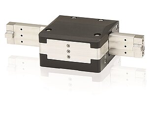
PI’s Piezo positioning systems use frictionless, wear-free flexure guides for that purpose. Repeatability in the single digit nanometer range is feasible and enables new applications such as the nanoimprinting process for structuring prototype wafers and small batch quantities as an alternative to the traditional lithographical process. Another nano-manufacturing application: 3-D laser lithography where piezo XYZ scanning stages precisely position the material to be exposed.

"Around 90% of all Smartphones..."
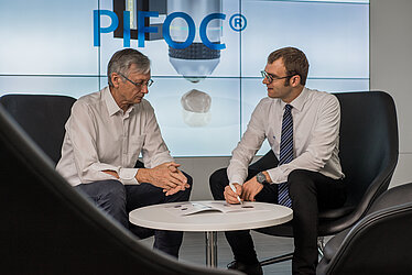
"... are manufactured with semiconductor processes that rely on our technology” explains Dr. Harry Marth, Head of Piezo Technology Innovation at PI (Physik Instrumente).
“We have grown together with the semiconductor and photonics sector and today our technology is represented in a large number of applications. Starting in the 1980s, the semiconductor industry pushed us to develop motion systems with nanometer resolution. The feature sizes kept getting smaller and the demand for piezo nanopositioning systems kept growing."
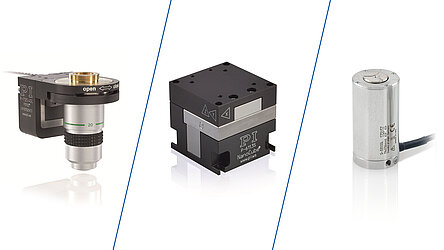
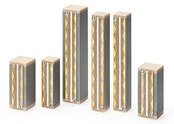
The piezo ceramic actuator is the driving force and one of the key ingredients in each nanopositioning system, in addition to sensors, guiding mechanisms, control algorithms and software.
What makes PI's Piezoelectrics Special
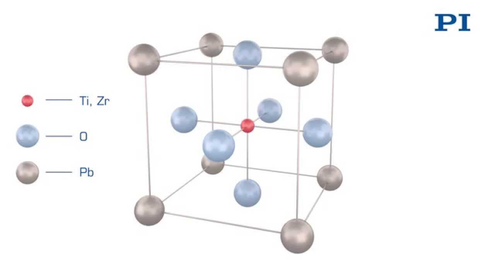
PI started designing and manufacturing its own piezo ceramics based on special PZT (Pb[ZrxTi1-x]O3) formulations at its, Lederhose, Thuringia site in 1990. After the reunification with the GDR, PI hired a number of experienced material scientists in this area and founded PI Ceramic.
"Over the decades, we have learnt how piezo ceramics behave and how to tune its different ingredients. We use this wealth of data for modeling when we design new systems. Having access to the piezo material and manufacturing technology puts PI in a very special position compared to other providers of precision motion systems. Large industrial ceramics manufacturers don’t focus on actuator-type ceramics, it’s only a niche for them ", says Dr. Marth and explains why this is a competitive advantage. What about Chinese competitors? "Not all piezo materials are created equal. Lighters and buzzers usually work with cheap piezo ceramics from Asia. Our key applications are in industrial precision motion with the highest demands on performance and lifetime. Obviously there are counterfeit products but our main competitors come from the USA and Japan", reports Dr. Marth, who has been working with the technology for more than 35 years.
A reward: The SEMI Technology Innovation Showcase Award was presented to PI for an innovative drive technology, called PiezoWalk® based on coordinated motion of multiple piezo actuators. The customers demand even more: There's no place for production downtimes in the semiconductor industry. As a precaution, companies are more inclined to change components beforehand in order to prevent downtimes. "That does not always make economic sense" says Dr. Marth.
The Intelligent Piezo goes Digital
That's one of the reasons why the researchers at PI want to make piezo drives even more intelligent. "Soon, each piezo will have its own IP address", jokes Dr. Mathias Bach, Head of Piezo Systems at Physik Instrumente.
Just a joke? His statement has a grain of truth: "Each piezo motion system reacts to temperature, humidity and air pressure. We want to record and analyze these environmental influences to develop lifetime models or even perform remote maintenance. We basically need to integrate a micro weather station with each piezo actuator. Smaller is usually better when it comes to nanopositioning systems", says Dr. Bach.
From Computer Chips to Tooling Machines
Tooling machine manufacturers are also showing interest in the technology.
Example: Electrical discharge machining (EDM): Adding piezo induced vibration to a rotary spindle moves particles generated by the EDM process out of the way cutting machining times by up to 60%.
"Another application is found in laser beam steering– special piezo mechanisms hold the position precisely, even after an emergency stop – in contrast to traditional positioning systems", explains Dr. Bach. "Simply self-locking", the physicist adds.
The applications of piezo technology are endless, however, not all design engineers are familiar with them and need to be educated before considering these non-traditional mechanisms. Nevertheless, the results from the semiconductor industry serve as an excellent reference.
