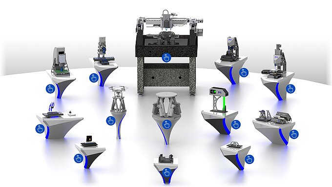
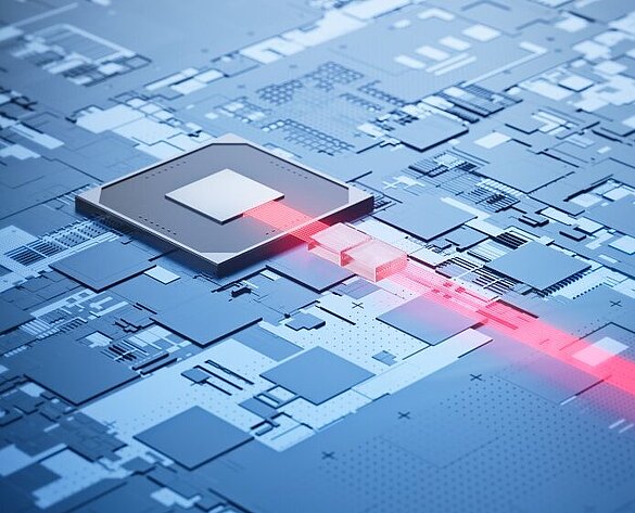
The photonics industry is clearly trending towards rapidly increasing production scale, with three orders of magnitude expected in the near future. Whether the challenge is economical, scalable manufacturing of multichannel silicon photonic (SiPh) devices, assembling increasingly sophisticated miniature cameras, or transmitting high-speed data across thousands of miles of space: Alignment is crucial for effectiveness, performance, and practicality. As photonics increasingly includes end-consumer and point-of-care applications, wearables will become a commodity. LIDAR and ADAS cameras are arguably the most important requirements for driverless vehicles. And there are many more applications on the horizon in quantum optics, optical computing, and more. To satisfy the need for photonics components in all these markets, intelligent automation of photonics test and assembly processes is required. The most time-consuming production step lies in the alignment of optics, fiber arrays, waveguides, or other photonic components. This is where new automated solutions will pay the biggest dividends with respect to yield, time-to-market, cost reduction, and rapidly scaling production volumes.
The crucial process of optical alignment is entrusted to generic positioners and rudimentary automation techniques that were developed as early as the 1980s and are still employed today for lack of more productive alternatives. As a result, the industry has had to cope with tedious, costly, poorly reproducible couplings and persistently poor yield, productivity, and scalability—until now. Modern mechanisms, equipped with advanced controls featuring intelligent, built-in alignment >> algorithms for automated and simultaneous optimization across multiple channels and degrees of freedom, can achieve complex alignments rapidly. Tasks that previously took minutes using legacy tools can now be completed with a single command, often in significantly less than a second. Let's explore the evolution of alignment methods, from manual processes to the sophisticated techniques of today.
Historical Photonics Alignment: Legacy Tools and Their Limits
Unsurprisingly, the first alignment automation tools accepted for production utilization came shortly after the advent of the personal computer in the late 1980s. These approaches used alignment functionality residing in software on the PC and were patiently executed in a stepwise, point-by-point manner. They were bottlenecked by the processing power and communication buses of the era, the plodding nature of then-contemporary motion controllers and stages, and the elementary capability of the algorithms. Still, they represented a multifold improvement in production economics compared with manual approaches, even with the dawn of low-cost manufacturing in Asia at the time. These approaches remain in wide use today, benefiting from the inertia of past acceptance.
That inertia, however, is soon to be swamped by the avalanche of demand from all the new SiPh applications. Multicore processors exist in more than just computers (even today’s Raspberry Pi has four powerful 64-bit cores), and PCs are no longer limited to 640 KB of memory and a few megabytes of storage. This has opened the door to considerably more sophisticated algorithms that in some cases even incorporate machine-learning functionalities.
The result is a suite of functionalities implemented as built-in, autonomous algorithms that operate with unprecedented speed at the submicron scale to address the challenges of SiPh and other photonic device testing and assembly processes. These challenges include:
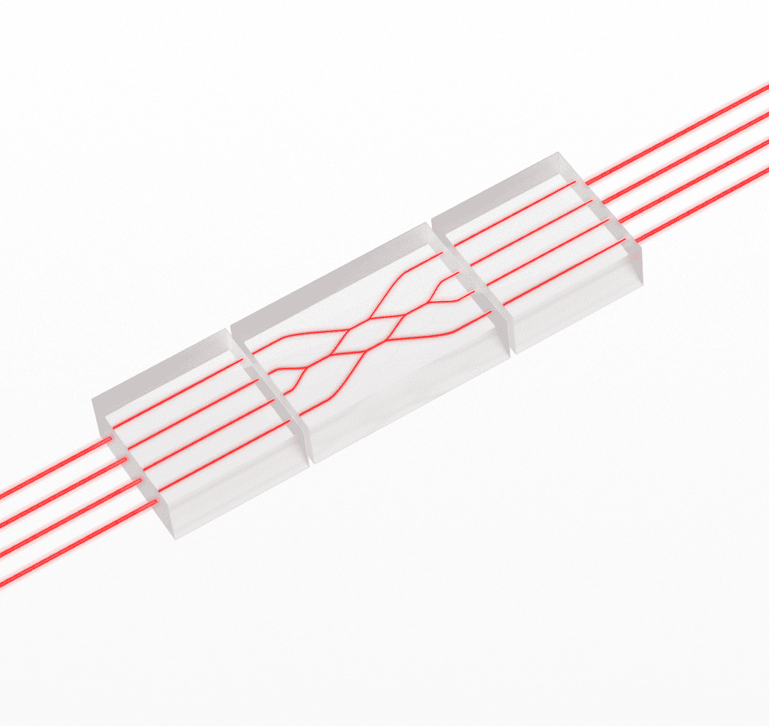
- Addressing the multi-channel nature of silicon photonic devices, which necessitate optimization in degrees of freedom (DOFs) far beyond those required in the simple pigtailing applications of the 1990s
- Parallel processing of optimization across channels, I/Os and DOFs, achieving consensus optimization across all of these in one step, versus the time-consuming serial sequence of steps required by legacy approaches
- A hundredfold improvement in overall alignment time
- Broad applicability across the fields of silicon photonics, imaging optics, lasers, and other electro-optic testing and assembly
With alignment comprising the lion’s share of the cost of a packaged SiPh device or optical assembly, the challenge is no small one in terms of production economics.
Fiber-Optic Alignment
To achieve maximum performance in fiber-optic alignment or photonics alignment, the components and tolerances involved are extremely small, sometimes on the order of a few dozen nanometers. Accuracy on this level requires mechanisms with submicron to nanometer resolution. In a typical SiPh manufacturing process, such alignments may be required up to two dozen times, starting with wafer testing and proceeding through multiple device assembly and test steps.
Passive vs. Active: Which Is the Future of Photonics Alignment?
Passive alignment relies on predetermined features implemented with extraordinary precision during the subcomponent fabrication process enabling Lego-like assembly of subcomponents, while active alignment uses high-precision motion and real-time feedback to optimize virtually any coupling. The choice between passive and active alignment depends on factors such as precision requirements, fabrication capabilities, system complexity, and cost considerations.
What is Passive Alignment?
Passive alignment refers to the process of aligning optical components within a system using mechanical fixtures, or predetermined alignment features. The process relies heavily on the inherent mechanical precision of alignment features to achieve accurate alignment. Passive alignment can be simple and cost-effective; it can work well enough when tolerances are less critical than those needed for most of the latest silicon photonics components. But in the general case, with the level of precision required for today’s high-performance photonic devices, it leads to increased costs, unreliable manufacturing processes, and low yield.
The hunt for passive alignment solutions has been underway for more than three decades, driven by the high per-piece costs imposed by manual and legacy active alignment approaches. Unfortunately, the need for nanoscale fabrication precision and reproducibility has limited the practicality of passive alignment for the general case. As an example, arrays of V-grooves can in theory be fabricated with the necessary precision. This has proved challenging in practice, and market trends in array channel count, format, and density throw fresh obstacles in the way of these implementations. Clever solutions to specific problems, such as >> Teramount’s Photonic Plug, have emerged and provide brilliant answers for tough use cases. For the more general case, the new availability of flexible, scalable active alignment suitable for today’s devices relieves the urgency to implement passive alignment approaches. An important factor in this is that active alignment does not rely on additional optical elements, mode expansion, or other tools needed in the passive-alignment toolbox.
Even with the very latest passive alignment techniques, some device tolerances such as fiber-core centration remain challenging. Additionally, it is hard to imagine how test processes requiring high-precision but temporary alignments—such as >> wafer probing and partial-assembly testing—could use passive alignment. It is for these reasons that the need for active alignment persists.

Precision alignment of individual components is essential in almost all industrial test and assembly processes to ensure proper functionality of the final product, boost the yield of the process, and achieve competitive quality metrics—note Elon Musk’s famous “10 micron” challenge to Tesla’s manufacturing team for panel gap consistency. This is especially true for optical modules, elements, and devices that must be aligned precisely to achieve rated performance and production yield. In advanced applications such as silicon photonics wafer probing, there is no alternative to active alignment.
Multiple channels, multiple elements, multiple interacting inputs and outputs, across multiple degrees of freedom, all need to be aligned and optimized multiple times in the manufacturing process. Finally, the anticipated need to scale for production volumes 1,000 times higher than today and the need to adapt to ever-shorter innovation cycles necessitated successful implementation of high-throughput precision alignment. Active alignment is the solution for efficient automation—with substantial cost savings.
What is Active Alignment?
Active alignment employs actuation (a computer-controlled precision stage or, in the simplest form, the hands of an operator turning knobs) and feedback from an optical power meter providing exact data regarding optical power and thus the coupling efficiency. With automated active alignment, the hands and eyes of the operator are replaced by a digital controller and an alignment algorithm that automatically drives the positioning mechanism until a given threshold or maximum optical power is achieved. Many solutions still implement algorithms in the PC, 1987-style. By comparison, the most advanced active alignment implementation is fully integrated into the controller for maximum speed and dependability.
Attaining Automated Active Alignment
One aspect most new photonics applications have in common is huge volumes compared with telecommunication and data-center applications. It is estimated that the industry must scale by a factor of 1,000 in just a few years. No manual process can scale like that—high-speed automation is essential. Alignment automation in some form has been used for more than thirty years. As devices grew smaller and more complicated, however, alignment times increased exponentially. Aligning a multi-lens assembly is far more demanding than aligning one with only two elements. Furthermore, attaching a silicon photonic chip with thirty-two channels takes significantly more time than pigtailing a laser diode, which was the big application in 1997. Ideally, multiple alignments across multiple elements and multiple degrees of freedom can be performed simultaneously in one quick step. This one-step process replaces multiple lengthy, repetitive loops required by legacy alignment technologies in these multichannel circumstances, reducing alignment times by two orders of magnitude.
Modern automated active alignment systems get the job done significantly faster than any manual operator can, and with higher repeatability. Although such systems require a higher initial investment, they offer flexibility, speed, and tremendous cost savings for large-quantity production. The latest systems can even optimize coupling performance across multiple channels and degrees of freedom simultaneously, which is crucial for silicon photonics applications with multiple circuits on a single chip. This approach speeds up >> testing and assembly, eliminating reliance on specialized labor and reference tolerances.
Silicon photonics structures require alignment accuracies between twenty and fifty nanometers to achieve the common 0.02 dB coupling repeatability specification, calling for novel motion technologies with even higher resolution. By actively controlling the alignment process, these systems compensate for subcomponent, fixturing, and placement tolerances, achieving higher levels of precision and repeatability compared with both passive alignment and older-method active alignment. Along with ensuring optimal performance, automated active alignment increases throughput and reduces costs.
Modern Mechanisms and Algorithms for Smart Fiber Alignment
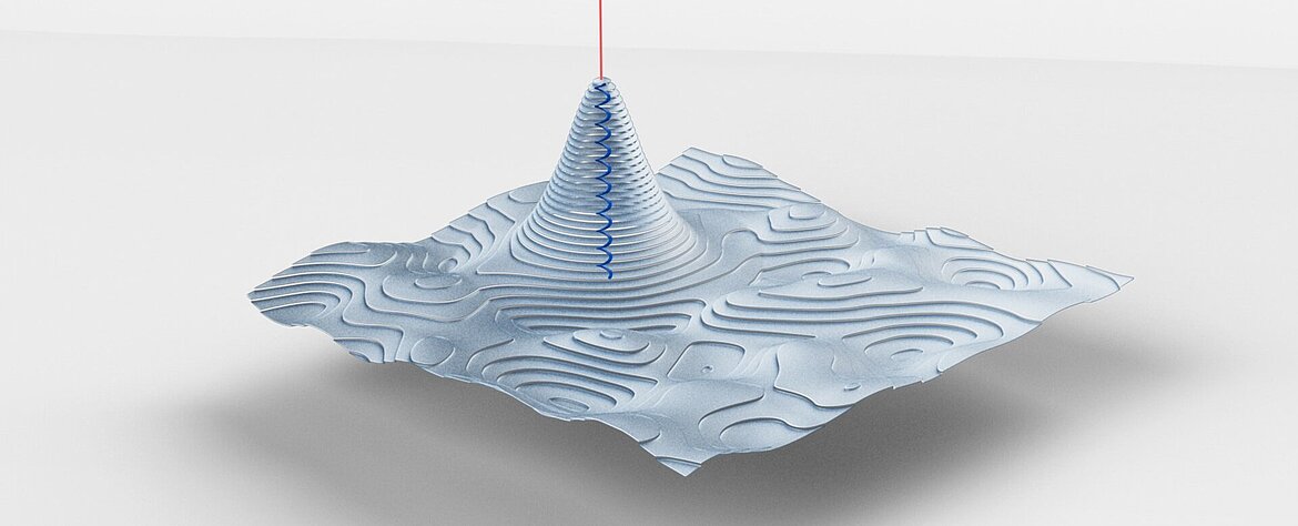
The very first automated alignment mechanisms required either special-purpose mechanisms or stacks of high-cost stages. Nearly a decade ago, new solutions based on combinations of multi-axis piezo nano positioning stages and hexapods proved suitable for new and emerging applications in >> SiPh testing and assembly. Most recently, cost-effective stacks of industrial stages were enabled through controller advancements to perform high-throughput, multichannel parallel alignment, forming an unprecedentedly flexible architecture that could even be applied to large substrates such as PCBs. Compact assemblies of air bearing axes bring their renowned cleanliness to the field. This addresses a key point of emerging concern, as it is recognized that “back end” processes such as probing and assembly for SiPh devices must be considerably cleaner compared with conventional microelectronics if yield targets are to be achieved. Finding first light, for example, has been a time-consuming procedure in all industrial photonics alignment applications, including wafer probing and device packaging. It is particularly time-consuming, though, in devices with inputs and outputs where both sides must be lined up for even a threshold amount of coupling to be achieved. That was the case up until now: